Improved far-UVC LEDs: investigations reveal causes of unwanted UVA radiation
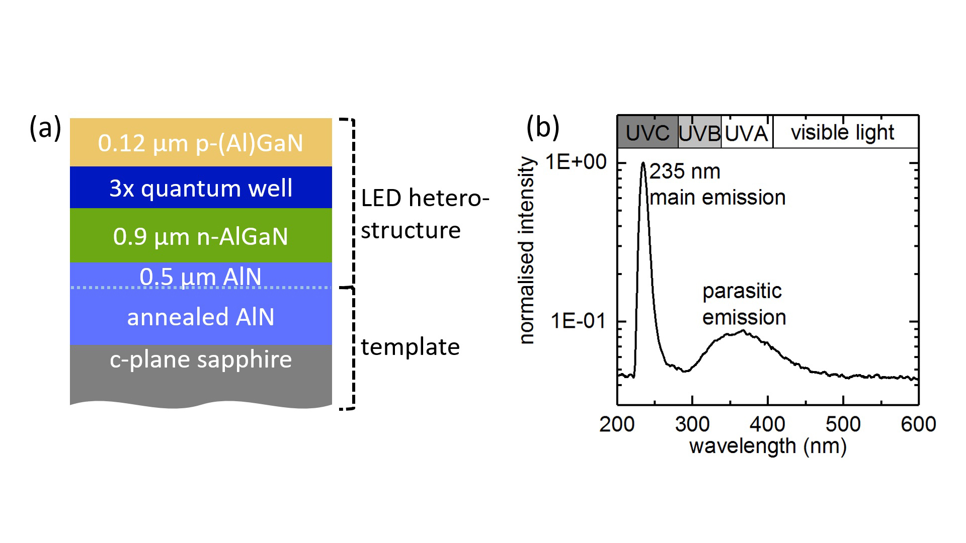
Fig. 1: Simplified schematic cross-section of a UVC LED heterostructure (a). Normalized room temperature on-wafer EL spectrum of a 235 nm UV LED heterostructure (b).
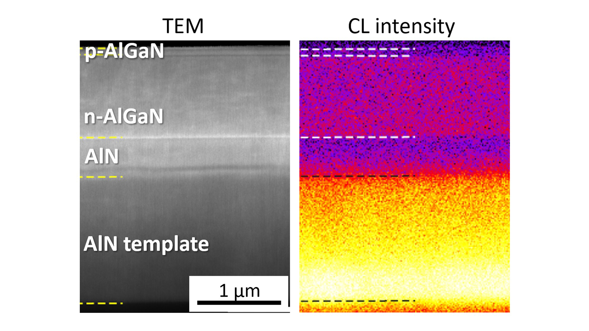
Fig. 2: TEM image of the far-UVC LED heterostructure and corresponding spectrally integrated CL intensity distribution.
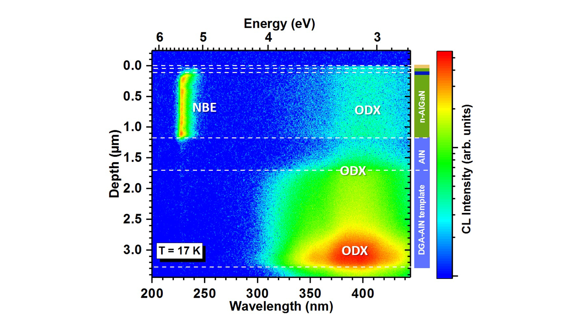
Fig. 3: Near band edge emission (NBE) and oxygen related point defects (ODX) identified by a CL-line scan along the cross section of the LED heterostructure.
AlxGa1-xN-based ultraviolet (UV) light emitting diodes (LEDs) are requested for a wide range of applications, e.g., disinfection, water purification, and medical treatments. Especially far-UVC LEDs with still relatively low efficiency compared to their longer wavelength counterparts may suffer from considerable loss of emission power due to the excitation of point defects. The radiative recombination via such point defects leads to parasitic emission. This not only causes a reduction in the emission power of the LEDs at the targeted wavelength, but some applications also require a spectrally pure light source. Recently, FBH and its collaborators have shown that far-UVC LEDs can effectively disinfect human skin, while longer wavelength components of the emission spectrum damage living cells. It is therefore important to understand where exactly the parasitic luminescence comes from in order to target its suppression.
UVC LEDs are commonly grown on AlN/sapphire templates in more or less complex heterostructures (Fig. 1a). At FBH, we use templates annealed at high temperatures prior to the heterostructure growth to improve the material quality. The emission spectrum of a far-UVC LED heterostructure emitting at 235 nm on such a template typically shows parasitic UVA emission (Fig. 1b). We investigated the origin of the emission in collaboration with the Otto-von-Guericke Universität Magdeburg, where powerful transmission electron microscopy (TEM) investigation methods are available. The cross-section of the LED heterostructure was imaged with high spatial resolution by a combination of TEM and cathodoluminescence (CL) generated by the focused electron beam. In this way, we obtained a detailed image of the heterostructure cross-section (Fig. 2a) and simultaneously the corresponding luminescence intensity distribution (Fig. 2b). To determine the spectral evolution of the emission in growth direction, we also took a spectrally resolved CL line scan from a cleaved cross-section of the LED (Fig. 3). From the spatial distribution of different wavelengths, the bright emission in the AlN template layer (Fig. 2b) can be assigned to an oxygen-related defect (ODX). Such defects were also detected in the n-AlGaN layer. The main origin of the UVA parasitic emission thus stems from point defects associated with oxygen in the AlN template and the n-AlGaN layer.
In further experiments, we also applied TEM-CL to far-UVC LED heterostructures grown on different AlN/sapphire templates. We found that the manufacturing method of the AlN/sapphire template and the defect density of the template can change the formation energy of point defects during heterostructure growth. Now that the causes of unwanted defect emission in far-UVC LEDs are known, targeted changes can be made to the manufacturing process.
This work was partially funded by the Federal Ministry of Education and Research (BMBF) within the “CORSA-Far-UVC” project (contract no. 03COV10E). The partners at Otto-von-Guericke Universität Magdeburg gratefully acknowledge the German Research Foundation (DFG) for financial support within the Research Instrumentation Program INST 272/148-1.
Publication
S. Hagedorn, T. Kolbe, G. Schmidt, F. Bertram, C. Netzel, A. Knauer, P. Veit, J. Christen, M. Weyers, "Origin of the parasitic luminescence of 235 nm UVC LEDs grown on different AlN templates", accepted for publication in Applied Physics Letters Dec. 2023.