Advanced in-situ etch depth control for dry etching processes – to achieve optimum device perfor-mance
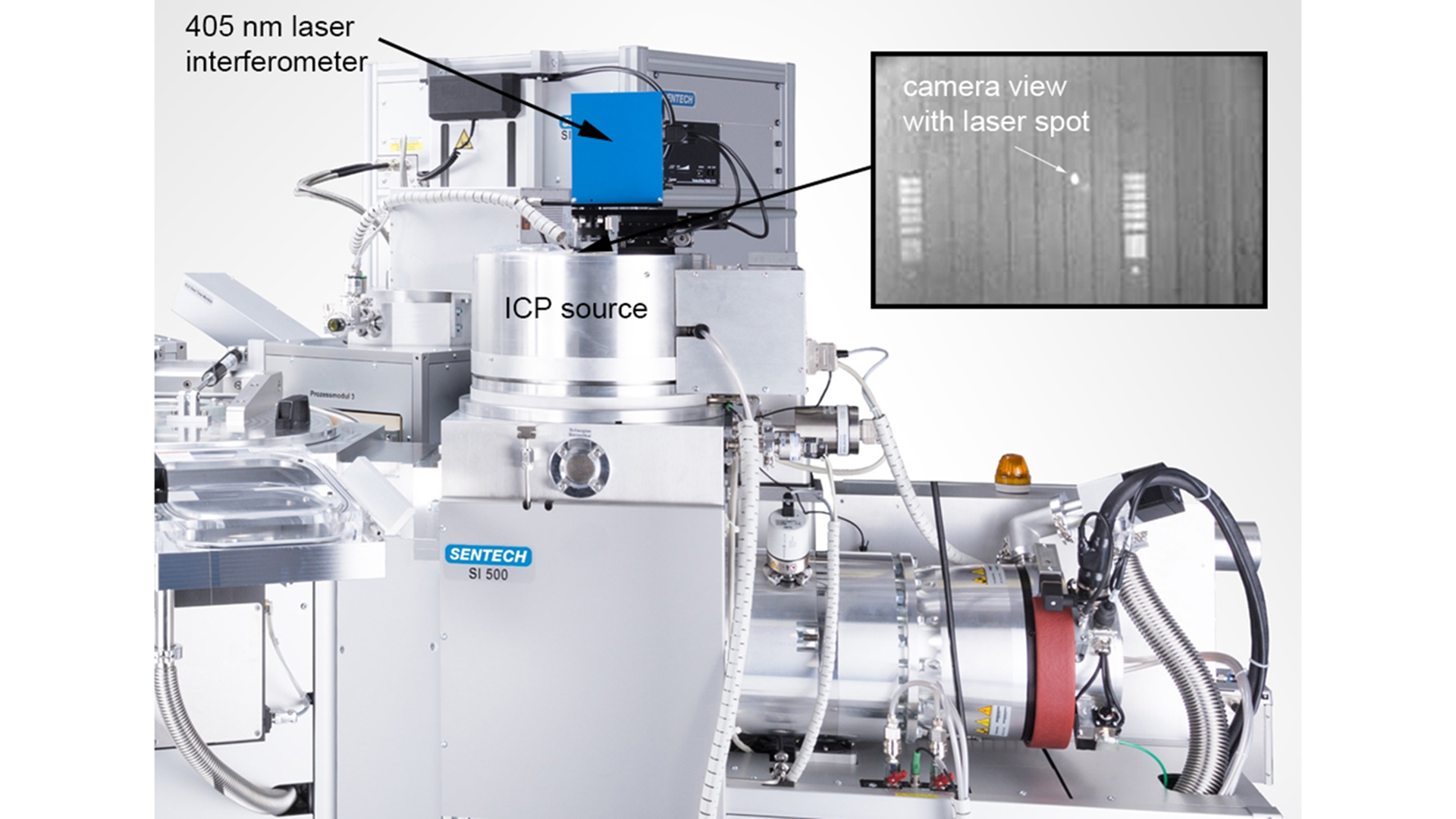
Fig 1: ICP etching system SI 500 with integrated laser interferometer operating at a measuring wavelength of 405 nm. Before starting the dry etching process, the position of the laser spot must be adjusted to the exposed area of the wafer, which is visible in the camera view shown in the inset.
Fig. 2: Reflected intensities of etch processes of two samples with identical epitaxial structure: sample #1 (blue line) was deeper etched than sample #2 that was etched to target depth, i.e., etching stopped after 7.2 periods (orange line). The number of periods was determined based on a simulation shown in the upper left part.
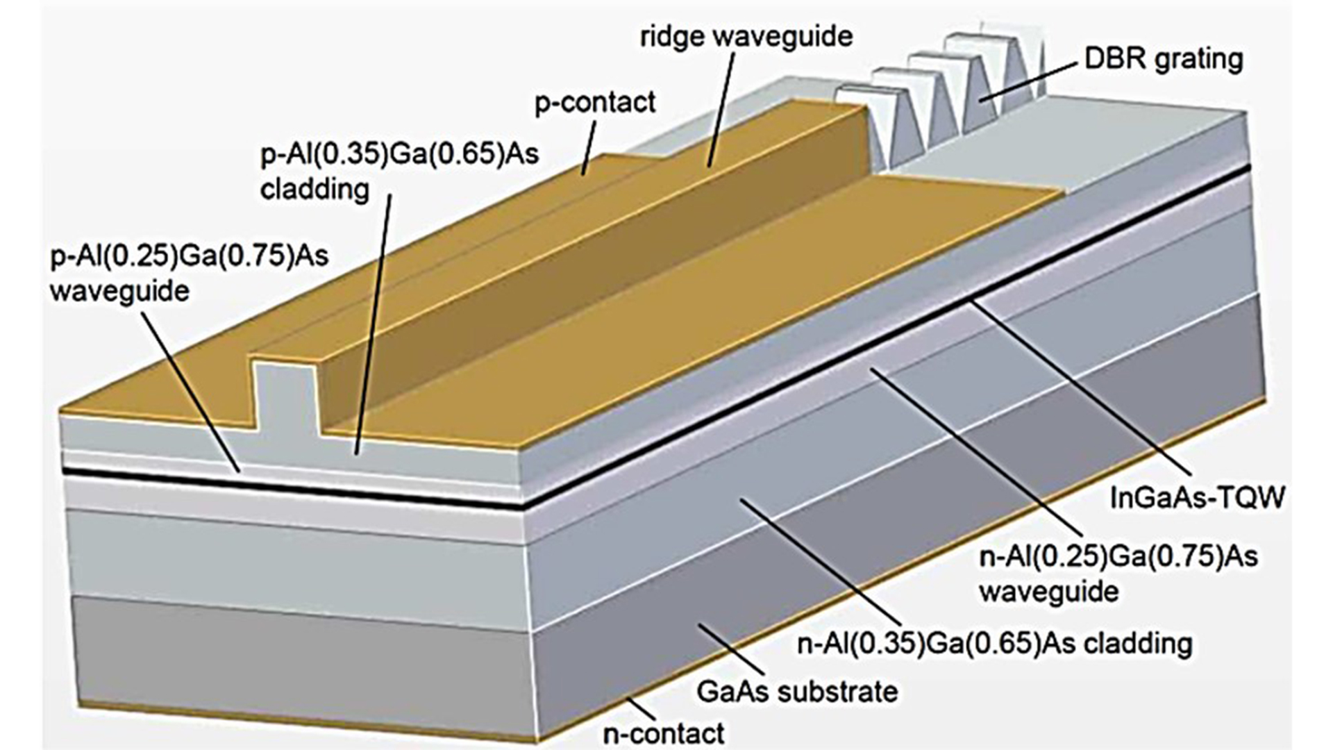
Fig. 3: Schematic layout of a DBR laser. Light is emitted below the ridge waveguide from the cleaved facet in the active area of the quantum wells (red arrow). To fabricate these lasers, well-controlled etching processes were used to form the contact planes, the waveguide ridges, and the DBR surface gratings [2].
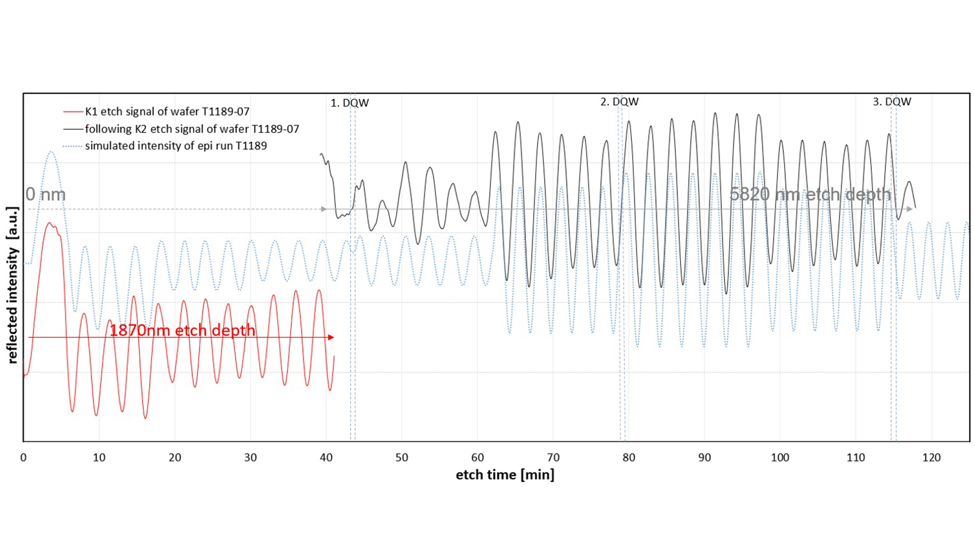
Fig. 4: The reflected intensity recorded from two successive reactive ion etching steps for etching the contact layers K1 and K2 is shown together with the simulation of the epitaxial stack. By simulating the entire epitaxial stack, it is possible to predict and control the etching depth. This enables precise stopping at the K1 target etch depth of 1870 nm before etching through the double quantum well (DQW1) and in a separate etch run at the K2 target etch depth of 5820 nm.
Developing high-power laser diodes requires highly precise dry etching processes to obtain a narrow bandwidth of the light as well as a high beam quality and stability. To obtain etch depth precision within a few nanometer ranges, we apply in-situ laser interferometry at FBH. The measurement method is based on interference of thin films. It generates a back-reflected signal that oscillates in time during etching. This is due to destructive and constructive interference from reflection at the layer interfaces and the etched surface. For complex layer structures, the expected intensity needs to be simulated. Since reflectivity and transparency are material properties of the semiconductor layers to be etched, the wavelength at which the laser interferometer should operate must be adapted to ensure optimum process control.
To account for the different epitaxial stacks to be etched, the etching tools are equipped with laser interferometers using different laser wavelengths, e.g., 405 nm for AlGaN/GaN and 980 nm for AlGaAs/InGaAs/GaAs epitaxial structures. Fig. 1 shows an SI 500 etch chamber with an in-situ measurement system on top of the ICP source. The 405 nm laser beam is directed through a sapphire window in the reactor lid onto the wafer surface. It is monitored by a camera and displayed to adjust the position of the measurement spot (see inset in Fig. 1). To monitor the etch depth during an etching process, the intensity reflected from the measurement spot is recorded and compared in-situ to the curve expected from simulations.
A challenging task when fabricating violet or blue emitting AlGaN/GaN-based laser diodes [1] is to precisely stop plasma etching once an electron blocking layer is reached. For such shallow etching steps in GaN-based epitaxial layers we apply an interferometer using 405 nm measurement wavelength. This wavelength leads to more interference periods per etching depth, i.e., a better accuracy, compared to systems operating at longer wavelengths. Furthermore, the high contrast of refractive indexes within the semiconductor heterostructure at 405 nm results in a high amplitude of the interference oscillations.
Fig. 2 shows the curves of the reflected signal recorded during the etching of two samples with identical epitaxial layer structures. It demonstrates a controlled etching process based on the simulation. Sample #1 (blue) was purposely etched deeper. Etching of sample #2 (orange) was stopped after 7.2 periods when reaching the electron blocking layer (EBL) layer at 570 nm depth. The number of periods (7.2) to obtain the target depth was determined by the simulation shown in the upper left corner. Due to the counting of interference periods, changes in the etch rate, as indicated by alterations of the periods of sample #1 compared to sample #2, do not affect the result. This is because the etch target is precisely achieved, and etching through the EBL is effectively prevented. A cross-sectional SEM image shown in the upper right part proves the right etching depth.
In contrast to GaN-based laser diodes, GaAs-based laser diodes exhibit strong light absorption at wavelengths below 600 nm, thus requiring a longer measurement wavelength. For this, we use a laser-interferometer operating at 980 nm. Fig. 3 shows a schematic of an AlGaAs/InGaAs/GaAs-based DBR laser. There are two critical etching processes that require in-situ depth control: First, the formation of the ridge waveguide while precisely reaching the p-contact epitaxial layer and second, the fabrication of the DBR grating. To fabricate the laser ridge for waveguiding, successive etch steps are required to etch through the cladding of the waveguide and through multiple quantum wells consisting of AlGaAs/InGaAs layers. We use a reactive ion etch (RIE) process at low RF power based on BCl3 and Cl2 gas in a dedicated etch chamber to obtain good selectivity to the photoresist mask at the rather long etching times of up to 80 minutes.
Fig. 4 shows an example of simulated and recorded intensity oscillations of the reflected signal at 980 nm during etching of two successive etching steps. We performed the two etching steps by counting the periods. The first etching was stopped after 12.1 etching periods at the target etching depth of 1870 nm, derived from simulation. The second etching was performed after preparation of another photoresist mask and stopped after further 26.1 periods at the target depth of 5820 nm.
To summarize, we use laser interferometry with different measurement wavelengths for precise in-situ process control of dry etching steps of the wide variety of epitaxial materials at FBH. Here, we aim to find a good compromise between higher precision achievable at lower wavelengths and maintaining sufficient material transparency for deeper etching obtained at higher wavelengths.
This work was partly funded by the German Federal Ministry of Education and Research (BMBF) within the framework of "Forschungsfabrik Mikroelektronik Deutschland (FMD)" under ref. 16FMD02.
Publications
[1] J. H. Kang, H. Wenzel, E. Freier, V. Hoffmann, J. Fricke, O. Brox, M. Matalla, and S. Einfeldt, “Continuous-wave operation of 405 nm distributed Bragg reflector laser diodes based on GaN using 10th-order surface gratings”, Photonics Research Vol. 10, Issue 5, pp.1157-1161 (2022)
[2] J. Fricke, W. John, A. Klehr, P. Ressel, L. Weixelbaum, H. Wenzel and G. Erbert, “Properties and fabrication of high-order Bragg gratings for wavelength stabilization of diode lasers”, Semicond. Sci. Technol. 27 055009 (2012)