Vertical high-voltage GaN-based pn-diodes on foreign and native substrates – targeting next-generation power electronics
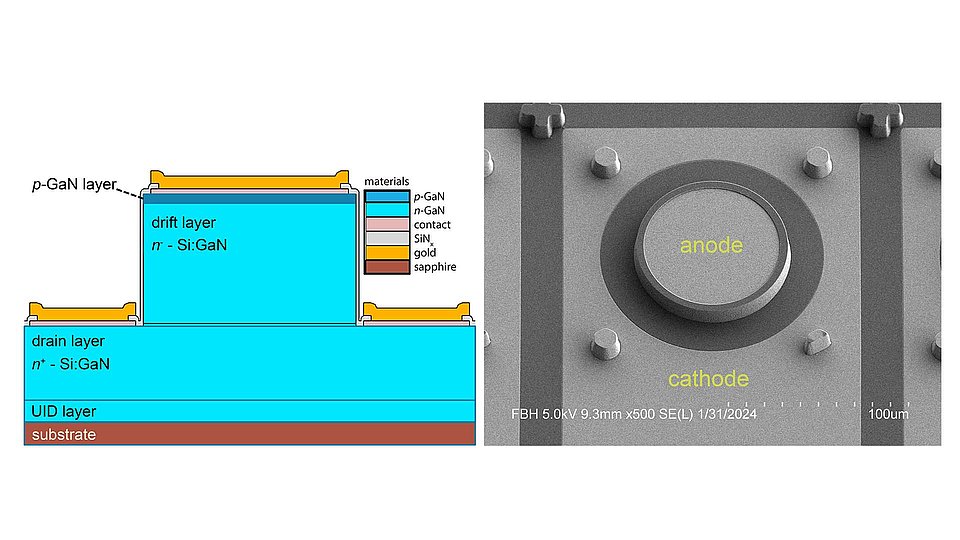
Fig. 1. Left: Schematic of the layer structure and layout of the quasi-vertical pn-diode and right: SEM picture of the processed circular device.
Vertical GaN‑based power switching devices are desired for their high blocking strength above 1.2 kV, while maintaining specific on‑state resistances lower than 1 mW×cm2. Both properties are key for power electronic converters with high power density and efficiency. However, achieving both features simultaneously is contradictive but can be optimized by careful design. Thus, growth of a GaN epitaxial drift region thicker than 10 µm with well controlled low carrier concentration as low as 1016 cm‑3 is required. Homoepitaxy on a free-standing GaN wafer allows growth of very thick layers due to an identical crystal constant and thermal expansion coefficient. Yet, free-standing GaN substrates, manufactured by Hydride Vapor Phase Epitaxy (HVPE) or ammonothermal (Am‑GaN) growth methods, feature a small diameter, have limited availability, and are very expensive. Alternatively, thick epitaxial GaN layers may be grown on commonly used sapphire substrates, which provide a large area and are attractively priced.
Growth of thick GaN epitaxial layers on sapphire substrates is not free from challenges. Strong lattice mismatch and large thermal expansion coefficient between the substrate and the GaN layer result in large wafer deformation, layer cracking, and propagation of structural defects to the epitaxial structures. Such growth anomalies deteriorate wafer processability in semiconductor process‑lines and the devices’ desired electrical properties. The epitaxial GaN layers quality grown on the different substrates can be quantified with their threading dislocation density (TDD). Typical threading dislocation density values are ~104 cm‑2, ~106‑107 cm‑2, and ~5×108 cm-2 for Am-GaN, HVPE, and sapphire substrates, respectively.
At FBH, we have developed thick epitaxial layers that serve as drift region in vertical GaN‑based power switching devices on different substrate types. The epitaxial structure comprises a 10 µm thick drift region and ~1-1.5×1016 cm-3 n-type doping concentration along with a specific resistivity of 1‑1.5 mW×cm2 grown by metal‑organic vapor phase epitaxy (MOVPE) on each of the substrate types. Quasi‑vertical pn‑diodes were manufactured as a sensitive electronic monitoring device to assess the drift zone properties. Fig. 1 depicts a GaN-based vertical diode scanning electron microscope micrograph and its schematic cross section.
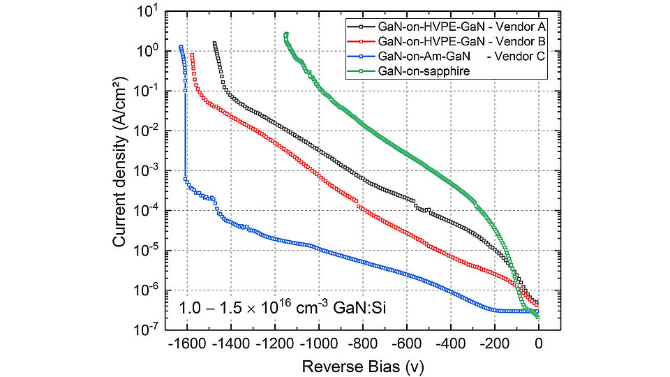
Characterizing these devices electrically provides validated information on the drift region conductivity, its exact carrier concentration, and its breakdown voltage. Namely, we investigated the relation between the threading dislocation density and the pn‑diode reverse blocking characteristics. Fig. 2 summarizes the reverse blocking characteristic of diodes manufactured on the different substrates. Diodes on Am-GaN substrates have the lowest reverse current and reach breakdown at ~1600 V. The IV characteristics at breakdown indicate avalanching. The reverse leakage current of diodes manufactured on HVPE substrates is two orders of magnitude higher and breakdown is reached at ~1450‑1550 V, still with indications for avalanching. On the other hand, the sapphire‑based diodes with the same drift zone doping level and thickness is limited to ~1100 V only due to an even higher leakage current level. In that case our current limit defining breakdown is reached prior to the onset of impact ionization. By comparing different types of substrates, we could deduct a direct correlation between threading dislocation density in the GaN drift layer with the reverse bias current and breakdown strength in pn‑diodes.
This work was partly supported by ECSEL JU through the European Union’s Horizon 2020 Research and Innovation Program and Germany, France, Belgium, Austria, Sweden, Spain, and Italy, under Grant 101007229. Further funding was provided by the Federal Ministry of Economics and Climate Protection (BMWK.IIB5) under reference 03EN4033E, joint project 01247760/1 – HoverGaN.
Publications
[1] E. Brusaterra, E. Bahat Treidel, F. Brunner, M. Wolf, A. Thies, J. Würfl, O. Hilt, “Optimization of vertical GaN drift region layers for avalanche and punch-through pn-diodes”, IEEE Electron Device Letters, vol. 44, no. 3, pp. 388-391, doi: 10.1109/LED.2023.3234101 (2023).
[2] E. Bahat Treidel, E. Brusaterra, M. Wolf, F. Brunner, O. Hilt, J. Würfl, “Drift region epitaxy development and characterization for high blocking strength and low specific resistance in vertical GaN based devices”, Proc. CS MANTECH, Orlando FL. USA, (2023).
[3] F. Brunner, E. Brusaterra, E. Bahat Treidel, O. Hilt, M. Weyers, “GaN drift layers on sapphire and GaN substrates for 1.2 kV class vertical power devices”, Phys. Status Solidi RRL, 2400013, doi: 10.1002/pssr.202400013 (2024).
[4] E. Brusaterra, E. Bahat Treidel, F. Brunner, A. Külberg, M. Wolf, O. Hilt, “Wafer Bow Tuning with Stealth Laser Patterning for Vertical High Voltage Devices with Thick GaN Epitaxy on Sapphire Substrates”, CS MANTECH, Tucson Az. USA (2024).
[5] E. Brusaterra, E. Bahat Treidel, F. Brunner, A. Külberg, M. Wolf, O. Hilt, “Comparison between sapphire and GaN substrates for 1.2kV rated vertical GaN pn-diodes”, MRS spring meeting, Seattle Wa. USA. (2024).

